
Researchers from Twente and Utrecht have made strips of germanium atoms that are one atom thick and a few nanometres wide. The two-dimensional nanoribbons have properties that could be useful in future quantum computers, the authors report in Nature Communications.
Germanene is a two-dimensional layer of germanium atoms just one atom thick, comparable to graphene, which is made up of carbon atoms. Researchers at the University of Twente and Utrecht University have now produced extremely thin strips of germanene, just a few nanometres wide.
Because of their unique structure, these so-called nanoribbons function as two-dimensional topological insulators: although the inside behaves as an insulator, electricity can flow along the edges without any energy loss. And as physicist and PhD student Dennis Klaassen from the University of Twente discovered, in the thinnest nanoribbons, which are only two to three atoms wide, these so-called topological edge states give way to even more special properties. Klaassen: ‘This came as a complete surprise.’
Heating and cooling
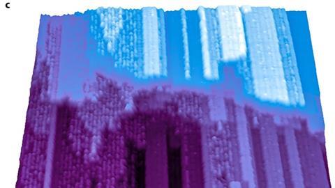
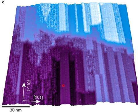
The researchers grew the nanoribbons on a rectangular germanium substrate. ‘The substrate has to be squeaky clean’, says Klaassen. To achieve this, they first bombarded the surface with argon ions in a vacuum system. Thanks to their high energy, these ions removed the top layers of atoms from the substrate. The researchers then deposited an atomically thin layer of platinum atoms on the substrate and heated the system to over 800°C. ‘As the substrate cooled, the germanium atoms crept up through the surface and formed a layer of germanene’, says Klaassen.
The fact that the germanium atoms form nanoribbons is due to the differences between the crystal lattices of platinum and germanene. The germanene lattice does not fit well into the platinum lattice in terms of width, says Klaassen. ‘Because germanene fits in the longitudinal direction, narrow, long structures are formed. The width of these nanoribbons varied between one and ten nanometres in our experiments.’
Disappearing edge states
The researchers expected the nanoribbons to have topological edge states. They confirmed this experimentally using a scanning tunneling microscope (STM). This instrument uses an extremely sharp metal needle, ideally only one atom thick at the tip. By applying a voltage difference between the needle and the surface, electrons can tunnel between them - the quantum phenomenon in which particles can bridge a distance despite a potential barrier.
The tunnel current generated depends on the distance between the needle and the surface. ‘By scanning the surface with the needle and measuring the tunnel current, the STM can determine where the nanoribbons are’, says Klaassen. ‘When the needle hits a nanoribbon, it measures an increased tunnel current and the device knows that the needle needs to be raised slightly.’
Using a similar method, the researchers were able to measure the electronic structure of the nanoribbons. ‘At the edge states, more electrons are available for tunneling, which is why we measured a higher tunnel current there than in the centre of a nanoribbon’, says Klaassen.
But contrary to expectations, Klaassen discovered a mysterious lower limit during the measurements: the edge states disappeared in nanoribbons more narrow than two nanometres. A phase transition seemed to have occurred in these nanoribbons, which are only a few atoms wide and are therefore called one-dimensional. ‘When we happened to make a measurement at the ends of one of these one-dimensional ribbons, we discovered that we could measure a state with a higher tunnel current.’
Quantum applications
The so-called end states of the one-dimensional nanoribbons are said to be correlated with each other - or, in quantum terms, entangled. This means that if something happens to the state at one end of the nanoribbon, it automatically affects the state at the other end.
Both the properties of two-dimensional and one-dimensional nanoribbons are useful for quantum computing. In two-dimensional nanoribbons, the edge states can be switched on and off by applying an electric field. ‘This makes them useful for energy-efficient, faster and smaller transistors’, says Klaassen.
The one-dimensional nanoribbons are particularly interesting for use as error-free quantum bits (qubits). In principle, the nanoribbons should be resistant to local defects, such as a missing atom or a disruption in the crystal lattice. ‘If you change the state at one end, the state at the other end of the nanoribbon should also change, provided the states are entangled’, says Klaassen. ‘However, this cannot be measured with our current STM. To confirm this, we will need to make measurements with multiple needles.’
Klaassen, D.J. et al. (2025) Nat. Commun. 16, DOI: 10.1038/s41467-025-57147-4


Nog geen opmerkingen