Computing at the speed of light, that is what optical computing is all about. The field is now experiencing a real revival thanks to the huge leap in the technical ability to design and manufacture materials at the nanoscale. ‘Optical computing is so much faster.’
Metamaterials can perform analogue mathematical operations on optical signals, such as images composed of light waves. These materials are several orders of magnitude smaller than conventional optical signal processing using lenses, US professors Andrea Alú and Nader Engheta argued in Science in 2014. ‘Well-designed blocks of metamaterials can perform mathematical operations on the profile of incoming light waves as they pass through the block.’
Optical computing is faster and uses less energy than electronic computing. The input is an image, or a set of light waves, on which a mathematical operation is performed, and the output is another image: mathematics at the speed of light. But optical signal processing requires large, complex systems of lenses and filters. Electronic computing is more flexible: the same set of transistors can perform all kinds of different mathematical operations. Optical and electronic computing were developed in parallel in the 1960s. This technology took off because of the advantages of electronic computing (also called digital computing). Optical computing was left behind. Modern computers perform all calculations electronically.

But electronic computing is reaching its limits. The need for efficient computing power that consumes less energy is growing. The processing speed and energy efficiency of classical electronics is now a limiting factor for some new applications such as artificial intelligence, machine learning and autonomous vehicles. On the other hand, this need for electronic processing power has actually enabled materials processing at the nanoscale. We wanted to put our electronic circuits on smaller and smaller chips, and this drove developments in lithography. These developments opened up new possibilities for optical computing. ‘You no longer need bulky optical elements, which makes integration on a chip possible,’ says Andrea Cordaro, a junior researcher at AMOLF, in his PhD thesis.
‘You design the material in such a way that it performs a mathematical operation on the incoming rays of light’
Andrea Cordaro
For his PhD research in Albert Polman’s group, Cordaro designed, fabricated and demonstrated optical metamaterials. In physical experiments, he showed that his creations can perform mathematical operations on light - in other words, they can perform optical calculations. ‘You design the so-called angular response of the material so that it performs a mathematical operation on the incoming light rays.’ Ultimately, it comes down to how the material is shaped. Cordaro gives it a certain nanostructure that corresponds to the mathematical operation he wants to perform. His metamaterials consist of an alumina slide with a thin layer of silicon on top. ‘Silicon is the most important material in the semiconductor industry, so we know how to process it at the nanoscale. It has been studied more than any other material in the last 70 years, and that is a big advantage.’
Nanostructure
For his PhD research in Albert Polman’s group, Cordaro designed, fabricated and demonstrated optical metamaterials. In physical experiments, he showed that his creations can perform mathematical operations on light - in other words, they can perform optical calculations. ‘You design the so-called angular response of the material so that it performs a mathematical operation on the incoming light rays.’ Ultimately, it comes down to how the material is shaped. Cordaro gives it a certain nanostructure that corresponds to the mathematical operation he wants to perform. His metamaterials consist of an alumina slide with a thin layer of silicon on top. ‘Silicon is the most important material in the semiconductor industry, so we know how to process it at the nanoscale. It has been studied more than any other material in the last 70 years, and that is a big advantage.’
For simple mathematical operations, you can design the nanostructure yourself. Calculating the second derivative, for example, corresponds to a nanostructure of regular vertical lattices. Cordaro had to run simulations to find the best lattice thickness. Calculating the second derivative is necessary for edge detection in images, he explains. ‘Image processing software often needs to determine where the edge of objects is in an image, for example for augmented reality, autonomous driving or wireless diagnostics.’ In the clean room, Cordaro carved the required pattern into the silicon. ‘You use lithography to apply the structure that has come out of the simulations to the silicon. The machine prints the pattern with an electron beam, so you can design on the nanometre scale,’ he says. ‘You start with flat silicon, add a mask, the electron beam etches the negative space out of the mask, then you bombard it with ions to wash away the negative space and finally you remove the mask.’

Butterfly
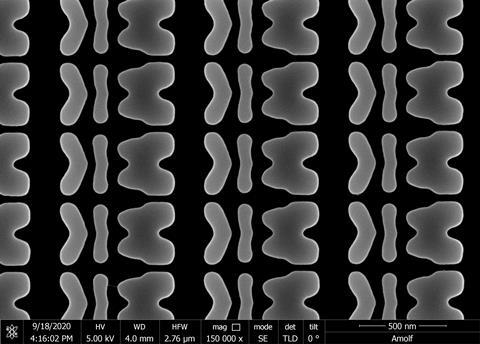
The nanostructure for edge detection proved that mathematical operations can be performed with a metamaterial. But for more complicated mathematical operations, the structure design is more difficult. Cordaro’s goal was to solve so-called Fredholm linear integral equations of the second kind. These are among the most common computational problems in research areas such as engineering, science and economics. This design is not intuitive, says Cordaro. So he used inverse design, or design in reverse, to find a suitable pattern. ‘You start with an objective and find a pattern that meets that objective. You send light through it on one side and then send back the ideal response. After several iterations, you find a local optimum.’
The shape he found for solving the integral equations looks like a butterfly, a flower or a fish, depending on who you ask, and is about 500 nm wide. Cordaro does not know why this is the right shape. Nor does he care. ‘It works! That is the most important thing to me. The simulated response is very close to the target.’ He printed the design back onto a silicon structure and demonstrated its operation. Last January, he published his findings in Nature Nanotechnology. He stresses that metamaterials will not replace electronic computing. ‘Transistors are flexible, that’s not going to change. But optical computing is much faster. You can combine optical and electronic components to reduce power consumption and increase speed. But at the moment it is not practical to make an all-optical computer.’
‘We won’t even have enough energy to keep up with how much we want to compute.’
Yoeri van de Burgt
Brain

Cordaro’s material is a great example of dedicated computing. Instead of a processor that can perform all tasks (a general-purpose machine), you make a specialised chip for a particular mathematical operation. Modern applications are moving towards specialised chips, says Yoeri van de Burgt, associate professor of microsystems at TU Eindhoven. The way we currently do computing is hopelessly inefficient, says Van de Burgt. A neural network has billions of connections between layers and nodes. You have to keep updating the values of the nodes until the result of the network has a certain value. ‘This updating is done sequentially. Ideally, you want the updating to happen in parallel, but an ordinary PC can’t do that.’ Our computing methods are not sustainable. ‘If we extrapolate our usage into the future, we will not have enough energy for the computing power we want.’

Patty Stabile, associate professor of electrical engineering at TU Eindhoven, is trying to mimic the brain to do optical computing on a chip. She explains how inefficient today’s supercomputers are compared to the human brain. ‘Artificial intelligence applications consume millions of watts. Our brains carry out that many operations per second, but they only consume a few tens of watts.’ She wants to recreate such a biological neural network on a photonic chip.
‘We need input from neuroscientists and they need a platform to test their theories’
Patty Stabile
The problem calls for a multidisciplinary approach. Besides mathematicians, physicists and materials scientists, you need neuroscientists who understand how the brain works. There are still many uncertainties. ‘We know some things, but not everything. We need input from neuroscientists and they need a platform to test their theories,’ says Stabile. She has already built a device that works and is configurable. In this device, she integrates linear and non-linear functions: the basic functions of a neural model. The challenge is to make it ultra-compact so that we can implement it on a large scale, and to find materials that are non-volatile, so that energy efficiency is high and she can implement more isomorphism.
It is unclear when and to what extent optical components will replace electronic ones. All data transport is already in the optical domain; only computing itself is still electronic. According to Van den Burgt, we need to be increasingly precise about what is needed where. ‘Some calculations can be done locally electronically, others locally optically. That is the revolution.’


Nog geen opmerkingen